STEM与日常科技·英语30篇(1)
4 / 30
正在确认阅读权限…
Why Semiconductor Cleanrooms Matter
半导体洁净室为什么重要
-
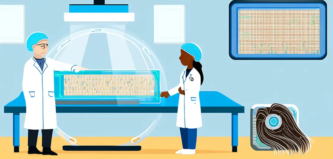
Modern microchips contain transistors smaller than 5 nanometers — about 1/10,000 the width of a human hair.
-
A single speck of dust larger than a transistor could break an entire circuit pattern during photolithography.
-
Cleanrooms use advanced air filtration, positive pressure, and strict gowning protocols to limit particles to fewer than 10 per cubic meter.
-
Workers wear full-body suits, gloves, masks, and shoe covers to prevent skin flakes, hair, or fibers from contaminating wafers.
-
Even airflow is carefully engineered: laminar flow pushes particles downward and away from sensitive silicon surfaces.
-
Vibrations, temperature swings, and static electricity are also tightly controlled, since they can distort nanoscale etching.
-
Without such environments, mass production of smartphones, medical scanners, or electric vehicle controllers would be impossible.
-
Each chip wafer passes through hundreds of steps across multiple cleanrooms — any contamination risks scrapping thousands of chips.